-
 Agriculture
-
 Health-Care
-
 Environment
-
 Construction-Real-Estate
-
 Tools-Hardware
-
 Home-Garden
-
 Furniture
-
 Luggage-Bags-Cases
-
 Medical-devices-Supplies
-
 Gifts-Crafts
-
 Sports-Entertainment
-
 Food-Beverage
-
 Vehicles-Transportation
-
 Power-Transmission
-
 Material-Handling
-
 Renewable-Energy
-
 Safety
-
 Testing-Instrument-Equipment
-
 Construction-Building-Machinery
-
 Pet-Supplies
-
 Personal-Care-Household-Cleaning
-
 Vehicle-Accessories-Electronics-Tools
-
 School-Office-Supplies
-
 Packaging-Printing
-
 Mother-Kids-Toys
-
 Business-Services
-
 Commercial-Equipment-Machinery
-
 Apparel-Accessories
-
 Security
-
 Shoes-Accessories
-
 Vehicle-Parts-Accessories
-
 Jewelry-Eyewear-Watches-Accessories
-
 Lights-Lighting
-
 Fabric-Textile-Raw-Material
-
 Fabrication-Services
-
 Industrial-Machinery
-
 Consumer-Electronics
-
 Electrical-Equipment-Supplies
-
 Electronic-Components-Accessories-Telecommunications
-
 Home-Appliances
-
 Beauty
-
 Chemicals
-
 Rubber-Plastics
-
 Metals-Alloys
- Masonry Materials
- Curtain Walls & Accessories
- Earthwork Products
- Fireproofing Materials
- Heat Insulation Materials
- Plastic Building Materials
- Building Boards
- Soundproofing Materials
- Timber
- Waterproofing Materials
- Balustrades & Handrails
- Bathroom & Kitchen
- Flooring & Accessories
- Tiles & Accessories
- Door, Window & Accessories
- Fireplaces & Stoves
- Floor Heating Systems & Parts
- Stairs & Stair Parts
- Ceilings
- Elevators & Escalators
- Stone
- Countertops, Vanity Tops & Table Tops
- Mosaics
- Metal Building Materials
- Multifunctional Materials
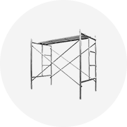
- Ladders & Scaffoldings
- Mouldings
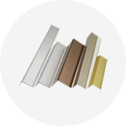
- Corner Guards
- Decorative Films
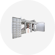
- Formwork
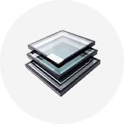
- Building & Industrial Glass
- Other Construction & Real Estate
- Wallpapers/Wall panels
- HVAC System & Parts
- Outdoor Facilities
- Prefabricated Buildings
- Festive & Party Supplies
- Bathroom Products
- Household Sundries
- Rain Gear
- Garden Supplies
- Household Cleaning Tools & Accessories
- Lighters & Smoking Accessories
- Home Storage & Organization
- Household Scales
- Smart Home Improvement
- Home Textiles
- Kitchenware
- Drinkware & Accessories
- Dinnerware, Coffee & Wine
- Home Decor
- Golf
- Fitness & Body Building
- Amusement Park Facilities
- Billiards, Board Game,Coin Operated Games
- Musical Instruments
- Outdoor Affordable Luxury Sports
- Camping & Hiking
- Fishing
- Sports Safety&Rehabilitation
- Ball Sports Equipments
- Water Sports
- Winter Sports
- Luxury Travel Equipments
- Sports Shoes, Bags & Accessories
- Cycling
- Other Sports & Entertainment Products
- Artificial Grass&Sports Flooring&Sports Court Equipment
- Scooters
- Food Ingredients
- Honey & Honey Products
- Snacks
- Nuts & Kernels
- Seafood
- Plant & Animal Oil
- Beverages
- Fruit & Vegetable Products
- Frog & Escargot
- Bean Products
- Egg Products
- Dairy Products
- Seasonings & Condiments
- Canned Food
- Instant Food
- Baked Goods
- Other Food & Beverage
- Meat & Poultry
- Confectionery
- Grain Products
- Feminie Care
- Hair Care & Styling
- Body Care
- Hands & Feet Care
- Hygiene Products
- Men's Grooming
- Laundry Cleaning Supplies
- Travel Size & Gift Sets
- Room Deodorizers
- Other Personal Care Products
- Pest Control Products
- Special Household Cleaning
- Floor Cleaning
- Kitchen & Bathroom Cleaning
- Oral Care
- Bath Supplies
- Yellow Pages
- Correction Supplies
- Office Binding Supplies
- Office Cutting Supplies
- Board Erasers
- Office Adhesives & Tapes
- Education Supplies
- Pencil Cases & Bags
- Notebooks & Writing Pads
- File Folder Accessories
- Calendars
- Writing Accessories
- Commercial Office Supplies
- Pencil Sharpeners
- Pens
- Letter Pad/Paper
- Paper Envelopes
- Desk Organizers
- Pencils
- Markers & Highlighters
- Filing Products
- Art Supplies
- Easels
- Badge Holder & Accessories
- Office Paper
- Printer Supplies
- Book Covers
- Other Office & School Supplies
- Stationery Set
- Boards
- Clipboards
- Stamps
- Drafting Supplies
- Stencils
- Electronic Dictionary
- Books
- Map
- Magazines
- Calculators
- Baby & Toddler Toys
- Educational Toys
- Classic Toys
- Dress Up & Pretend Play
- Toy Vehicle
- Stuffed Animals & Plush Toys
- Outdoor Toys & Structures
- Balloons & Accessories
- Baby Food
- Children's Clothing
- Baby Supplies & Products
- Maternity Clothes
- Kids Shoes
- Baby Care
- Novelty & Gag Toys
- Dolls & Accessories
- Puzzle & Games
- Blocks & Model Building Toys
- Toddler Clothing
- Baby Clothing
- Kids' Luggage & Bags
- Arts, Crafts & DIY Toys
- Action & Toy Figures
- Baby Appliances
- Hobbies & Models
- Remote Control Toys
- Promotional Toys
- Pregnancy & Maternity
- Hygiene Products
- Kid's Textile&Bedding
- Novelty & Special Use
- Toy Weapons
- Baby Gifts
- Baby Storage & Organization
- Auto Drive Systems
- ATV/UTV Parts & Accessories
- Marine Parts & Accessories
- Other Auto Parts
- Trailer Parts & Accessories
- Auto Transmission Systems
- Train Parts & Accessories
- Universal Parts
- Railway Parts & Accessories
- Auto Brake Systems
- Aviation Parts & Accessories
- Truck Parts & Accessories
- Auto Suspension Systems
- Auto Lighting Systems
- New Energy Vehicle Parts & Accessories
- Auto Steering Systems
- Wheels, Tires & Accessories
- Bus Parts & Accessories
- Auto Performance Parts
- Cooling System
- Go-Kart & Kart Racer Parts & Accessories
- Air Conditioning Systems
- Heavy Duty Vehicle Parts & Accessories
- Auto Electrical Systems
- Auto Body Systems
- Auto Engine Systems
- Container Parts & Accessories
- Motorcycle Parts & Accessories
- Refrigeration & Heat Exchange Equipment
- Machine Tool Equipment
- Food & Beverage Machinery
- Agricultural Machinery & Equipment
- Apparel & Textile Machinery
- Chemical Machinery
- Packaging Machines
- Paper Production Machinery
- Plastic & Rubber Processing Machinery
- Industrial Robots
- Electronic Products Machinery
- Metal & Metallurgy Machinery
- Woodworking Machinery
- Home Product Manufacturing Machinery
- Machinery Accessories
- Environmental Machinery
- Machinery Service
- Electrical Equipment Manufacturing Machinery
- Industrial Compressors & Parts
- Tobacco & Cigarette Machinery
- Production Line
- Used Industrial Machinery
- Electronics Production Machinery
- Other Machinery & Industrial Equipment
- Camera, Photo & Accessories
- Portable Audio, Video & Accessories
- Television, Home Audio, Video & Accessories
- Video Games & Accessories
- Mobile Phone & Accessories
- Electronic Publications
- Earphone & Headphone & Accessories
- Speakers & Accessories
- Smart Electronics
- TV Receivers & Accessories
- Mobile Phone & Computer Repair Parts
- Chargers, Batteries & Power Supplies
- Used Electronics
- VR, AR, MR Hardware & Software
- Projectors & Presentation Equipments
- Other Consumer Electronics
- Cables & Commonly Used Accessories
- Computer Hardware & Software
- Displays, Signage and Optoelectronics
- Discrete Semiconductors
- Wireless & IoT Module and Products
- Telecommunications
- Connectors, Terminals & Accessories
- Development Boards, Electronic Modules and Kits
- Circuit Protection
- Sensors
- Isolators
- Audio Components and Products
- Integrated Circuits
- Power Supplies
- Relays
- RF, Microwave and RFID
- Electronic Accessories & Supplies
- Passive Components
- PCB & PCBA
- Air Quality Appliances
- Home Appliance Parts
- Heating & Cooling Appliances
- Small Kitchen Appliances
- Laundry Appliances
- Water Heaters
- Water Treatment Appliances
- Refrigerators & Freezers
- Personal Care & Beauty Appliances
- Major Kitchen Appliances
- Cleaning Appliances
- Second-hand Appliances
- Smart Home Appliances
- Other Home Appliances
- Energy Chemicals
- Inorganic Chemicals
- Basic Organic Chemicals
- Agrochemicals
- Admixture & Additives
- Catalysts & Chemical Auxiliary Agents
- Pigments & Dyestuff
- Coating & Paint
- Daily Chemicals
- Polymer
- Organic Intermediate
- Adhesives & Sealants
- Chemical Waste
- Biological Chemical Products
- Surface Treatment Chemicals
- Painting & Coating
- Chemical Reagents
- Flavor & Fragrance
- Non-Explosive Demolition Agents
- Other Chemicals
- Custom Chemical Services
Integrated Circuits
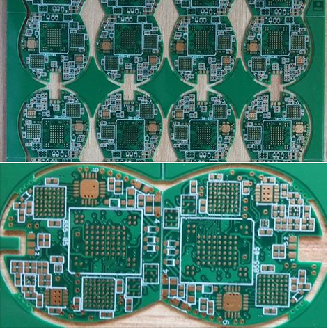
Efficient PCB Thermal Management Solutions
Understanding Heat Generation and Dissipation
Before delving into specific solutions, it's crucial to understand the sources and pathways of heat generation within a PCB. Heat is primarily generated by electronic components, such as microprocessors, power transistors, and integrated circuits (ICs), due to resistive losses and switching actions. The amount of heat generated depends on factors such as power consumption, ambient temperature, and the thermal resistance of the components themselves. Effective thermal management aims to efficiently transfer this generated heat away from these components to the surrounding environment, preventing excessive temperature rise.
Heat dissipation relies on several mechanisms: conduction, convection, and radiation. Conduction involves the transfer of heat through direct physical contact, while convection utilizes the movement of fluids (air or liquid) to carry heat away. Radiation involves the emission of thermal energy in the form of electromagnetic waves. Understanding these mechanisms is essential for designing effective thermal solutions, as they influence the choice of materials and strategies employed.
Heat Sinks and Thermal Pads
Heat sinks are passive devices designed to increase the surface area available for heat dissipation, significantly improving convective cooling. They are typically made of high-thermal-conductivity materials like aluminum or copper and are attached to heat-generating components. The design of a heat sink—its size, fin density, and surface finish—significantly impacts its effectiveness. Larger surface area generally leads to better cooling, but also increases size and weight. Fin density affects the balance between surface area and airflow resistance.
Thermal pads or interfaces are crucial for ensuring effective heat transfer between the heat-generating component and the heat sink. These materials fill gaps and irregularities, minimizing thermal resistance at the interface. Different materials offer varying thermal conductivities, allowing engineers to select the best option based on the application's thermal requirements and cost constraints. Choosing a pad with appropriate thermal conductivity and compressibility is vital for optimal performance.
Active Cooling Solutions
For high-power applications where passive cooling is insufficient, active cooling methods are necessary. These typically involve the use of fans to enhance convective cooling. Fans create forced airflow, accelerating the removal of heat from the heat sink. Careful selection of fan size, speed, and airflow characteristics is essential to ensure adequate cooling without introducing excessive noise or vibration.
Liquid cooling systems provide even more efficient heat removal, particularly for high-power density applications. These systems circulate a coolant (often water or a specialized fluid) through a network of channels or microchannels in contact with the heat-generating components. Liquid cooling offers superior heat transfer capabilities compared to air cooling, enabling the dissipation of significantly higher power densities. However, they are more complex and expensive to implement.
PCB Layout and Design Considerations
The physical layout of the PCB plays a significant role in its thermal performance. Components generating significant heat should be strategically placed to maximize airflow and minimize thermal coupling with sensitive components. Consideration should be given to trace routing and component placement to avoid hot spots and ensure even heat distribution. Using copper planes or thermal vias can help spread heat more evenly across the board.
Material selection is also important. Choosing PCB substrates with high thermal conductivity can significantly improve heat dissipation. Aluminum-based substrates or copper-clad laminates offer improved thermal performance compared to standard FR-4 materials. These choices, however, often come with increased cost and fabrication complexity.
Thermal Simulation and Analysis
Before prototyping and finalizing the PCB design, it is highly recommended to perform thermal simulations using specialized software. These simulations allow engineers to predict temperature distributions under various operating conditions, identifying potential hot spots and optimizing the thermal management strategy. This iterative design process, incorporating simulation results, helps to minimize thermal-related issues and ensure the reliability of the final product.
Careful monitoring of the PCB's thermal performance during operation is also crucial. Employing temperature sensors allows for real-time monitoring and early detection of potential overheating issues. This proactive approach allows for timely intervention and prevents catastrophic failure.

PCB Design Software A Comprehensive Overview
Schematic Capture
The design process typically begins with schematic capture, where the engineer creates a visual representation of the circuit's components and their interconnections. PCB design software provides intuitive interfaces with libraries of pre-defined components, allowing users to quickly assemble the circuit. These libraries often contain extensive parts databases, simplifying the selection and placement of components. Advanced features such as hierarchical design, enabling the breakdown of complex circuits into manageable sub-circuits, are also common. This modular approach greatly improves design organization and maintainability, particularly for large and intricate projects. Error checking features, such as design rule checks (DRC) at the schematic level, proactively identify potential issues before proceeding to the PCB layout, saving time and reducing costly revisions.
Furthermore, many software packages offer sophisticated simulation capabilities integrated directly within the schematic capture environment. This allows designers to verify the circuit's functionality through simulations before committing to physical layout, enabling early detection and correction of potential design flaws. These simulations can include various analyses such as SPICE simulations for analyzing circuit behavior under different conditions, helping to optimize performance and ensure robustness.
PCB Layout
Once the schematic is complete, the design moves to the PCB layout stage. This involves physically arranging the components on the board and routing the connections between them, a task demanding precision and attention to detail. PCB design software facilitates this process by providing tools for component placement, automated routing algorithms, and manual routing capabilities for intricate connections. The software's automated routing engines leverage sophisticated algorithms to optimize trace lengths, minimize signal interference, and adhere to specified design rules. However, manual intervention is often necessary for critical signal paths or complex routing scenarios, giving the designer fine-grained control over the layout. The user interface typically includes visual aids such as signal integrity analysis tools to help identify and mitigate potential signal quality issues.
Effective PCB layout also requires careful consideration of thermal management, especially for high-power applications. The software often integrates thermal analysis tools that predict temperature distributions on the board, allowing designers to optimize component placement and incorporate heat sinks or other thermal management solutions to prevent overheating and ensure reliable operation. Furthermore, the ability to create and manage multiple layers is crucial for complex designs, enhancing design flexibility and minimizing board size. Efficient layer management within the software ensures a clear and manageable design process.
Design Rule Checking (DRC) and Manufacturing Output
Design rule checking (DRC) plays a crucial role in ensuring the manufacturability of the PCB. The software performs automated checks against a set of predefined rules, ensuring that the design adheres to the limitations and requirements of the chosen manufacturing process. These rules include things like trace width and spacing, clearance between components, and minimum pad sizes. Identifying and correcting DRC violations early in the design process prevents costly manufacturing errors and delays. The software also generates a range of manufacturing-ready output files, including Gerber files, which are the industry-standard data format for PCB fabrication.
Beyond Gerber files, modern PCB design software often integrates with cloud-based manufacturing services, enabling seamless transitions from design to production. This streamlines the entire workflow, reducing lead times and facilitating collaboration between designers and manufacturers. Additionally, the software may include features for generating documentation such as bill of materials (BOM) and assembly drawings, streamlining the entire production process.
Advanced Features and Integrations
Beyond the core functionalities, many advanced PCB design software packages offer additional features to enhance design efficiency and capabilities. These may include features such as signal integrity analysis tools, electromagnetic field simulation capabilities, and support for high-speed design techniques. These advanced tools are crucial for designing high-performance PCBs for applications with stringent signal integrity requirements. Moreover, integration with other design tools, such as 3D modeling software, allows designers to visualize their PCB within the context of the larger system, improving integration and design verification.
The selection of PCB design software depends on factors such as design complexity, budget, and the specific needs of the project. While many free and open-source options exist, professional-grade software offers a richer feature set and more robust support for demanding projects. The continuous evolution of PCB design software reflects the ever-increasing complexity of modern electronic devices, constantly improving efficiency and enabling the creation of more innovative and powerful systems.

High Speed PCB Design Best Practices Guide
Signal Integrity Management
Signal integrity is paramount in high-speed designs. Maintaining signal integrity involves minimizing signal distortion and ensuring the signal arrives at its destination accurately and reliably. This necessitates careful consideration of impedance control, minimizing transmission line effects, and managing reflections. A significant portion of a High-Speed PCB Design Best Practices Guide would be dedicated to these issues, emphasizing the importance of controlled impedance routing for all critical signals. This involves using specific trace widths and spacing, controlled dielectric thickness, and proper stackup design to maintain a consistent characteristic impedance throughout the signal path.
Furthermore, the guide will likely stress the importance of minimizing stubs and via transitions. These abrupt changes in impedance can cause significant signal reflections, leading to signal degradation. Careful planning of signal routing and the strategic placement of vias are crucial to mitigate these issues. The guide would likely suggest using controlled impedance vias and techniques like minimizing via lengths and employing proper via stitching techniques to reduce the impact of via discontinuities.
Power Integrity and Decoupling
High-speed circuits are power-hungry and sensitive to noise. Power integrity, therefore, is just as crucial as signal integrity. A High-Speed PCB Design Best Practices Guide would extensively cover effective decoupling techniques to ensure a clean and stable power supply. This involves strategically placing capacitors of appropriate values and types close to the power pins of high-speed ICs. The guide would likely emphasize the importance of using multiple decoupling capacitors with varying capacitance values to cover a wide range of frequencies. This helps to suppress noise across the spectrum.
Beyond the placement of individual capacitors, the guide would also address the importance of a well-designed power plane. A continuous, low-impedance power plane acts as a reservoir of energy, smoothing out voltage fluctuations and reducing noise. The guide would provide recommendations on plane design, including minimizing plane discontinuities, optimizing plane size and shape, and ensuring sufficient current carrying capacity.
Layout Considerations and Routing
PCB layout is critical for high-speed designs. A poorly laid-out board can negate the benefits of careful signal integrity management. A High-Speed PCB Design Best Practices Guide would detail various aspects of PCB layout specifically tailored for high-speed applications. This would include guidance on routing strategies, such as minimizing trace lengths for high-frequency signals and employing controlled impedance techniques. The guide might also suggest specific routing styles, such as minimizing bends and using parallel routing for sensitive signals.
Furthermore, the guide would emphasize the importance of separating high-speed signals from noise-sensitive components and analog circuitry. This often involves creating distinct signal zones or using shielding techniques to prevent crosstalk and electromagnetic interference (EMI). Effective placement of ground planes and the use of guard traces are also often mentioned to ensure signal integrity.
Component Selection and Placement
The choice of components significantly impacts high-speed performance. A High-Speed PCB Design Best Practices Guide would highlight the importance of selecting components with appropriate characteristics for high-frequency operation. This would include considerations such as component tolerance, parasitic capacitance and inductance, and signal bandwidth. The guide would also likely advise on the use of surface mount technology (SMT) components, which generally offer better performance at higher frequencies compared to through-hole components.
Component placement is also crucial, with the guide emphasizing the importance of minimizing trace lengths, strategically placing decoupling capacitors close to integrated circuits, and ensuring sufficient spacing between components to minimize crosstalk and EMI. The placement of high-speed components often influences the overall PCB layout and routing strategy.
EMI/EMC Compliance
High-speed PCBs often emit electromagnetic radiation, potentially interfering with other electronic systems or failing to meet regulatory standards. A comprehensive High-Speed PCB Design Best Practices Guide would address EMI/EMC considerations throughout the design process. This includes guidelines for proper grounding, shielding techniques, and the use of EMI/EMC filters to mitigate unwanted emissions and susceptibility to external interference. The guide would emphasize the importance of conducting thorough simulations and measurements to ensure compliance with relevant standards.
Ultimately, a well-executed High-Speed PCB Design Best Practices Guide acts as a comprehensive reference for engineers, helping them to navigate the complex challenges of designing high-speed circuits. By following these best practices, designers can significantly improve signal integrity, reduce noise, and ensure their designs meet performance specifications, leading to reliable and robust products.
REPORT


